News
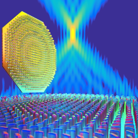
An illustration of the ultra-thin planar lens. The lens consists of titanium dioxide nanofins on a glass substrate. The lens focuses an incident light to a spot smaller than the wavelength this tight focusing enables subwavelength resolution imaging. (Image courtesy of Peter Allen/Harvard John A. Paulson School of Engineering and Applied Science)
Curved lenses, like those in cameras or telescopes, are stacked in order to reduce distortions and resolve a clear image. That’s why high-power microscopes are so big and telephoto lenses so long.
While lens technology has come a long way, it is still difficult to make a compact and thin lens (rub a finger over the back of a cellphone and you’ll get a sense of how difficult). But what if you could replace those stacks with a single flat — or planar — lens?
Researchers from the Harvard John A. Paulson School of Engineering and Applied Sciences (SEAS) have demonstrated the first planar lens that works with high efficiency within the visible spectrum of light — covering the whole range of colors from red to blue. The lens can resolve nanoscale features separated by distances smaller than the wavelength of light. It uses an ultrathin array of tiny waveguides, known as a metasurface, which bends light as it passes through.
The research is described in the journal Science.

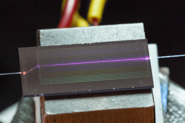
Light passing through the meta-lens is focused by millions of nano structures (Capasso Lab)
“This technology is potentially revolutionary because it works in the visible spectrum, which means it has the capacity to replace lenses in all kinds of devices, from microscopes to cameras, to displays and cell phones,” said Federico Capasso, Robert L. Wallace Professor of Applied Physics and Vinton Hayes Senior Research Fellow in Electrical Engineering and senior author of the paper. “In the near future, metalenses will be manufactured on a large scale at a small fraction of the cost of conventional lenses, using the foundries that mass produce microprocessors and memory chips.”
"Correcting for chromatic spread over the visible spectrum in an efficient way, with a single flat optical element, was until now out of reach," said Bernard Kress, Partner Optical Architect at Microsoft, who was not part of the research. "The Capasso group's metalens developments enable the integration of broadband imaging systems in a very compact form, allowing for next generations of optical sub-systems addressing effectively stringent weight, size, power and cost issues, such as the ones required for high performance AR/VR wearable displays."
In order to focus red, blue and green light — light in the visible spectrum — the team needed a material that wouldn’t absorb or scatter light, said Rob Devlin, a graduate student in the Capasso lab and co-author of the paper.
“We needed a material that would strongly confine light with a high refractive index,” he said. “And in order for this technology to be scalable, we needed a material already used in industry.”
The team used titanium dioxide, a ubiquitous material found in everything from paint to sunscreen, to create the nanoscale array of smooth and high-aspect ratio nanostructures that form the heart of the metalens.
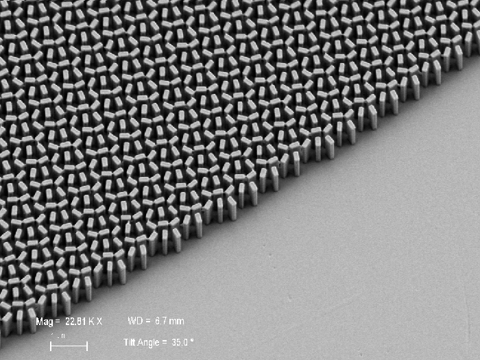
Scanning electron microscope micrograph of the fabricated meta-lens. The lens consists of titanium dioxide nanofins on a glass substrate. Scale bar: 2 mm (Image courtesy of the Capasso Lab)
“We wanted to design a single planar lens with a high numerical aperture, meaning it can focus light into a spot smaller than the wavelength,” said Mohammadreza Khorasaninejad, a postdoctoral fellow in the Capasso lab and first author of the paper. “The more tightly you can focus light, the smaller your focal spot can be, which potentially enhances the resolution of the image.”
The team designed the array to resolve a structure smaller than a wavelength of light, around 400 nanometers across. At these scales, the metalens could provide better focus than a state-of-the art commercial lens.
“Normal lenses have to be precisely polished by hand,” said Wei Ting Chen, coauthor and a postdoctoral fellow in the Capasso Lab. “Any kind of deviation in the curvature, any error during assembling makes the performance of the lens go way down. Our lens can be produced in a single step — one layer of lithography and you have a high performance lens, with everything where you need it to be.”
"The amazing field of metamaterials brought up lots of new ideas but few real-life applications have come so far," said Vladimir M. Shalaev, professor of electrical and computer engineering at Purdue University, who was not involved in the research. "The Capasso group with their technology-driven approach is making a difference in that regard. This new breakthrough solves one of the most basic and important challenges, making a visible-range meta-lens that satisfies the demands for high numerical aperture and high efficiency simultaneously, which is normally hard to achieve."
One of the most exciting potential applications, said Khorasaninejad, is in wearable optics such as virtual reality and augmented reality.
“Any good imaging system right now is heavy because the thick lenses have to be stacked on top of each other. No one wants to wear a heavy helmet for a couple of hours,” he said. “This technique reduces weight and volume and shrinks lenses thinner than a sheet of paper. Imagine the possibilities for wearable optics, flexible contact lenses or telescopes in space.”
The authors have filed patents and are actively pursuing commercial opportunities.
The paper was coauthored by Jaewon Oh and Alexander Zhu of SEAS. It was supported in part by a MURI grant from the Air Force Office of Scientific Research, Draper Laboratory and Thorlabs Inc.
Topics: Optics / Photonics
Cutting-edge science delivered direct to your inbox.
Join the Harvard SEAS mailing list.
Scientist Profiles

Federico Capasso
Robert L. Wallace Professor of Applied Physics and Vinton Hayes Senior Research Fellow in Electrical Engineering
Press Contact
Leah Burrows | 617-496-1351 | lburrows@seas.harvard.edu