News
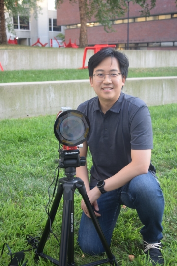
Joon-Suh Park with the 10-cm diameter meta-optic astro-imager. (Image courtesy of Joon-Suh Park)
Joon-Suh Park, a graduate student at the Harvard John A. Paulson School of Engineering and Applied Sciences (SEAS) and the Graduate School of Arts and Sciences (GSAS), has been named a DARPA Riser by the Defense Advanced Research Projects Agency (DARPA).
DARPA Risers are up-and-coming researchers whose work could have applications to national security and demonstrates the potential to lead to technological surprise. The Risers program provides early-career scientists the opportunity to be recognized for their work and present their ideas directly to DARPA leadership, program managers, and university faculty at the DARPA Forward conference.
At the conference, Park will be presenting his research on mass-producible, 10-centimeter glass metalenses that operate at the visible wavelength. The metalens consists of 18.7 billion sub-wavelength glass nanostructures and could be used for applications in space as well as terrestrial applications such as long-range imaging platforms.
As a member of Prof. Federico Capasso’s group at SEAS, Park is focused on designing and fabricating these large, mass-manufacturable metasurfaces. Park has helped develop techniques to fabricate lenses using lithography, the same technology currently used to manufacture silicon chips. The technique can produce many metalenses per chip, eliminating the time-consuming deposition processes required for previous metalenses by etching the nanostructure pattern directly onto a glass surface. Park is also working to understand the effects of fabrication errors, which are likely to arise during mass-manufacturing processes, on the optical performance of metalenses.
“A lens can image better in low-light imaging conditions if the size of the lens is increased,” said Park. “We have shown a path to creating a large diameter metalens that exceeds the exposure size limit of conventional lithography tools by demonstrating a 10-centimeter diameter metalens that can image in the visible spectrum.”
Park’s research paves the way for metalenses and chips to be fabricated by the same manufacturer and directly stacked on each other in devices such as cell phones and AR and VR systems.
“Our work can also be applied to low-payload requiring imaging platforms, such as for satellites or for unmanned aerial vehicles,” said Park.
To demonstrate the 10-centimeter diameter metalens' imaging capabilities, Park and the team took the first meta-optic image of space in the visible spectrum, imaging the North America Nebula and the Moon.
Before joining the Capasso group, Park served as a Research Scientist at Korea Institute of Science and Technology (KIST) for five years, where he worked on the design, fabrication and testing of optoelectronic devices ranging from solar cells, quantum dot photodetectors, quantum dot LEDs, quantum cascade lasers and various semiconductor fabrication techniques.
Topics: Applied Physics, Awards, Optics / Photonics
Cutting-edge science delivered direct to your inbox.
Join the Harvard SEAS mailing list.
Press Contact
Leah Burrows | 617-496-1351 | lburrows@seas.harvard.edu