News
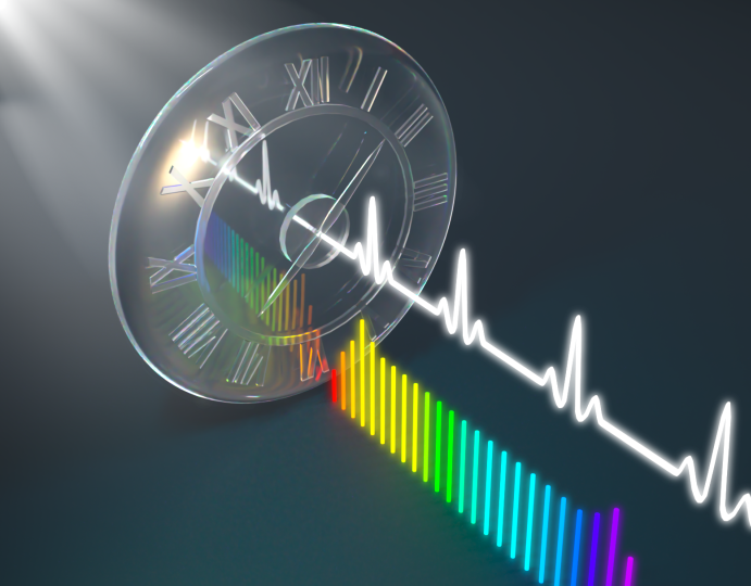
A time lens transforms a continuous-wave, single-color laser beam into a high-performance, on-chip femtosecond pulse source. (Credit: Second Bay Studios/Harvard SEAS)
Download ImageFemtosecond pulsed lasers — which emit light in ultrafast bursts lasting a millionth of a billionth of a second — are powerful tools used in a range of applications from medicine and manufacturing, to sensing and precision measurements of space and time. Today, these lasers are typically expensive table-top systems, which limits their use in applications that have size and power consumption restrictions.
An on-chip femtosecond pulse source would unlock new applications in quantum and optical computing, astronomy, optical communications and beyond. However, it’s been a challenge to integrate tunable and highly efficient pulsed lasers onto chips.
Now, researchers from the Harvard John A. Paulson School of Engineering and Applied Sciences (SEAS) have developed a high-performance, on-chip femtosecond pulse source using a tool that seems straight out of science fiction: a time lens.
The research is published in Nature.
“Pulsed lasers that produce high-intensity, short pulses consisting of many colors of light have remained large,” said Marko Lončar, the Tiantsai Lin Professor of Electrical Engineering at SEAS and senior author of the study. “To make these sources more practical, we decided to shrink a well-known approach, used to realize conventional – and large — femtosecond sources, leveraging a state of the art integrated photonics platform that we have developed. Importantly, our chips are made using microfabrication techniques like those used to make computer chips, which ensures not only reduced cost and size, but also improved performance and reliability of our femtosecond sources.”
Traditional lenses, like contact lenses or those found in magnifying glasses and microscopes, bend rays of light coming from different directions by altering their phase so that they hit the same location in space — the focal point.
Time lenses, on the other hand, “bend” light beams in similar ways – but they alter the phase of light beams in time rather than space. In this way, different colors of light, which travel at different speeds, are re-timed so that they each hit the focal plane at the same time.
Imagine a car race, in which each color of light is a different car. First, the time lens staggers the leave time of each car, then sets their speed so they arrive at the finish line at the same time.
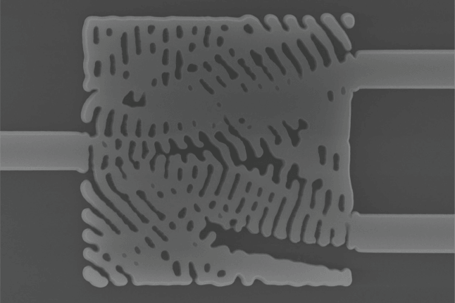
To generate femtosecond pulses, the team’s device uses a series of optical waveguides, couplers, modulators and optical grating on the lithium niobate platform pioneered by Lončar’s lab.
The team starts by passing a continuous-wave, single-color laser beam through an amplitude modulator that controls the amount of light going through the time-lens, a function similar to an aperture in a conventional lens. The light then propagates through the “bendy” part of the lens, a phase modulator in this case, where a frequency comb of different colors is generated. Going back to the car analogy, the phase modulator creates and then releases the cars of different colors at different starting times.
Then the final component of the laser comes in — a fishbone grating along the waveguide. The grating changes the speed of the different colors of light to bring them all in line with each other, neck and neck in the race, so that they hit the finish line (or focal plane) at the same time
Because the device controls how fast different wavelengths travel and when they hit the focal plane, it effectively transforms the continuous, single color laser beam into a broadband, high-intensity pulse source that can produce ultra-fast, 520 femtosecond bursts.
The device is highly tunable, integrated onto a 2cm by 4mm chip and, because of lithium niobate’s electro-optical properties, requires significantly reduced power than table-top products.
There’s no tradeoff here; you save energy at the same time you save space. You just get better performance as the device gets smaller and more integrated.

“We’ve shown that integrated photonics offers simultaneous improvements in energy consumption and size,” said Mengjie Yu, a former postdoctoral fellow at SEAS and first author of the study. “There’s no tradeoff here; you save energy at the same time you save space. You just get better performance as the device gets smaller and more integrated. Just imagine — in the future we can carry around femtosecond pulse lasers in our pockets to sense how fresh fruit is or track our well-being in real time, or in our cars to do distance measurement.”
Yu is currently an Assistant Professor at the University of Southern California.
Next, the team aims to explore some of the applications for both the laser itself and the time lens technology, including in lensing systems like telescopes as well as in ultrafast signal processing and quantum networking.
Harvard’s Office of Technology Development has protected the intellectual property arising from the Loncar Lab’s innovations in lithium niobate systems. Loncar is a cofounder of HyperLight Corporation, a startup which was launched to commercialize integrated photonic chips based on certain innovations developed in his lab.
The research was a collaboration between Harvard, HyperLight, Columbia University and Freedom Photonics.
The paper was co-authored by David Barton, Rebecca Cheng, Christian Reimer, Prashanta Kharel, Lingyan He, Linbo Shao, Di Zhu, Yaowen Hu, Hannah R. Grant, Leif Johansson, Yoshitomo Okawachi, Alexander L. Gaeta and Mian Zhang.
It was supported by the Defense Advanced Research Projects Agency (HR0011-20-C-0137), Army Research Office (W911NF2010248), Office of Naval Research (N00014- 18-C-1043) and Air Force Office of Scientific Research (FA9550-19-1-0376 and FA9550-20-1-0297).
Topics: Applied Physics, Technology
Cutting-edge science delivered direct to your inbox.
Join the Harvard SEAS mailing list.
Scientist Profiles
Marko Lončar
Tiantsai Lin Professor of Electrical Engineering
Press Contact
Leah Burrows | 617-496-1351 | lburrows@seas.harvard.edu