News
Researchers led by Marko Lončar at SEAS have managed to control the rate of emission of photons from diamond nanoposts, an important advance toward quantum computing.
Cambridge, Mass. – October 9, 2011 – Engineers and physicists at Harvard have managed to capture light in tiny diamond pillars embedded in silver, releasing a stream of single photons at a controllable rate.
The advance represents a milestone on the road to quantum networks in which information can be encoded in spins of electrons and carried through a network via light, one photon at a time.
The finding was published in Nature Photonics, appearing online on October 9.
“We can make the emission of photons faster, which will allow us to do more processing per second—for example, more computations—in the future quantum network,” explains principal investigator Marko Lončar, Associate Professor of Electrical Engineering at the Harvard School of Engineering and Applied Sciences (SEAS).
The device Lončar's research team has built consists of parallel rows of tiny, nanofabricated diamond posts, embedded in a layer of silver, that can each act as a single photon source.
By removing the silver wrapping from their nanostructures, the team was also able to achieve a slower release of photons, which is of interest for probing the dynamics of the quantum system.
The breakthrough takes advantage of imperfections in the diamond’s crystal lattice, where carbon atoms are replaced by other elements. To the naked eye, these imperfections can appear as discolorations in the diamond, turning it yellow in the case of nitrogen. Occasionally, there is also a vacancy (missing carbon atom) next to the nitrogen atom.
Each nitrogen-vacancy imperfection can serve as a nearly perfect quantum emitter, capable of emitting red photons one by one, even at room temperature. The technology is a promising candidate for realization of scalable, on-chip quantum networks.
“The color centers in diamond are very interesting as qubits for quantum information processing, where they can be used as memory to store information,” says Lončar. “More importantly, they can be interrogated—they can be written into and read out—with light.”
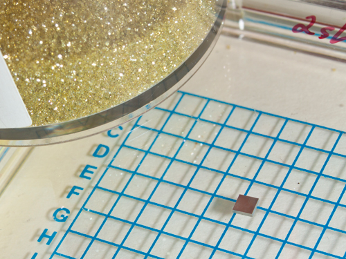
Imperfections in the diamond can give the crystals a characteristic color. Nitrogen in these tiny diamonds (top) turns them yellow. (Microdiamond powder provided by Daniel Twitchen and the Element Six company [UK].) Some imperfections, including the nitrogen-vacancies explored in this work, are luminescent (can emit red photons one at a time) and behave as excellent optically addressable quantum memory. The chip (bottom right) consists of diamond with a silver layer on top.
Lončar’s team fabricates diamond posts that contain negatively charged nitrogen vacancy centers, which can absorb light and hold its energy for a given amount of time, finally releasing it in the form of photons.
"The rate at which photons are emitted can be controlled by carefully nano-engineering the center’s surrounding," says co-author Irfan Bulu, a research associate in the Lončar group. Attaining fine control of that release, however, has been difficult.
“One of the main challenges has been the efficiency with which you can write information into the spin of these color centers, as well as the efficiency with which you can collect photons emitted from the color centers," explains co-author Jennifer Choy, a graduate student in Lončar’s lab at SEAS. "The other challenge has been the rate—how quickly you can perform these processes.”
Previous work from Lončar’s group solved the collection efficiency problem by using diamond nanowires to channel and direct the flow of photons. The new research manipulates the radius of diamond pillars and adds the silver coating. The diamond-silver construction acts as an optical nanoresonator, creating a strong electromagnetic field around the emitter and offering a new level of control over the rate of emission.
Moreover, the device functions at room temperature—an essential requirement for practical computing applications—and the nanostructured chips are fully scalable.
“We’ve designed everything in parallel in a massive system, which allows us to make thousands or millions of devices with more or less the same properties, and we use conventional microfabrication and nanofabrication techniques, unlike what has been done in this field before,” says Birgit Hausmann, a graduate student in Lončar’s lab at SEAS and one of the co-authors.
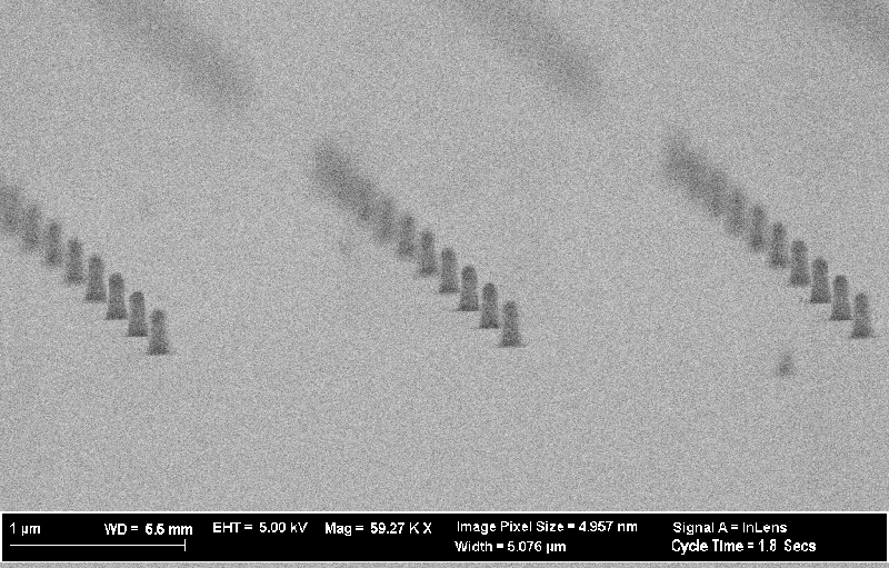
SEM image of the diamond nanoposts. Each one is approximately 100nm wide and 200nm tall. A nanometer is a billionth of a meter. Image courtesy of Jennifer Choy.
In addition to Lončar, Choy, Hausmann, and Bulu, co-authors included Tom Babinec, a graduate student at SEAS; Mughees Khan, a staff scientist at the Wyss Institute for Biologically Inspired Engineering at Harvard; Patrick Maletinsky, a fellow of the Department of Physics at Harvard; and Amir Yacoby, Professor of Physics in the Harvard Faculty of Arts and Sciences.
The work was supported by grants and fellowships from the U.S. Department of Defense, the Defense Advanced Research Projects Agency (DARPA) QuEST program, the National Science Foundation (NSF), the King Abdullah University of Science and Technology (KAUST), the Sloan Foundation, and the NSF-supported Nanoscale Science and Engineering Center (NSEC) at Harvard. Fabrication took place at the NSF-supported Center for Nanoscale Systems (CNS) at Harvard.
Cutting-edge science delivered direct to your inbox.
Join the Harvard SEAS mailing list.
Scientist Profiles

Marko Lončar
Tiantsai Lin Professor of Electrical Engineering

Amir Yacoby
Mallinckrodt Professor of Physics and of Applied Physics
Press Contact
Caroline Perry