News
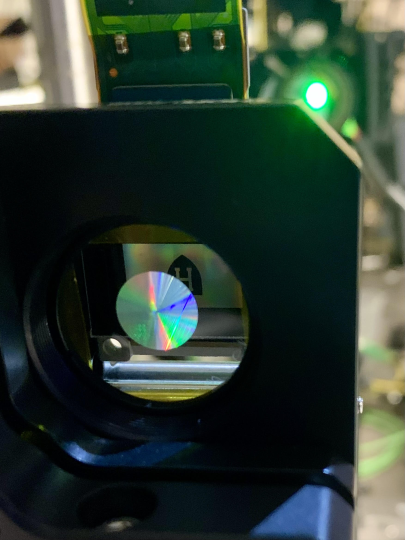
The fabricated metalens together with a micro-LCD display showing a Harvard logo. (Credit: Capasso Lab/Harvard SEAS)
Compact and lightweight metasurfaces — which use specifically designed and patterned nanostructures on a flat surface to focus, shape and control light — are a promising technology for wearable applications, especially virtual and augmented reality systems. Today, research teams painstakingly design the specific pattern of nanostructures on the surface to achieve the desired function of the lens, whether that be resolving nanoscale features, simultaneously producing several depth-perceiving images or focusing light regardless of polarization.
If the metalens is going to be used commercially in AR and VR systems, it’s going to need to be scaled up significantly, which means the number of nanopillars will be in the billions. How can researchers design something that complex? That’s where artificial intelligence comes in.
In a recent paper, published in Nature Communications , a team of researchers from the Harvard John A. Paulson School of Engineering and Applied Sciences (SEAS) and the Massachusetts Institute of Technology (MIT) described a new method for designing large-scale metasurfaces that uses techniques of machine intelligence to generate designs automatically.
“This article lays the groundwork and design approach which may influence many real-world devices,” said Federico Capasso, the Robert L. Wallace Professor of Applied Physics and Vinton Hayes Senior Research Fellow in Electrical Engineering at SEAS and senior author of the paper. “Our methods will enable new metasurface designs that can make an impact on virtual or augmented reality, self-driving cars, and machine vision for embarked systems and satellites.”
Until now, researchers needed years of knowledge and experience in the field to design a metasurface.
“We’ve been guided by intuition-based design, relying heavily on one’s training in physics, which has been limited in the number of parameters that can be considered simultaneously, bounded as we are by human working memory capacity,” said Zhaoyi Li, a research associate at SEAS and co-lead author of the paper.
To overcome those limitations, the team taught a computer program the physics of metasurface design. The program uses the foundation of physics to generate metasurface designs automatically, designing millions to billions of parameters simultaneously.
This is an inverse design process, meaning the researchers start with a desired function of the metalens — such as a lens that can correct chromatic aberration — and the program finds the best design geometries to achieve that goal using its computational algorithms.
“Letting a computer make a decision is inherently scary but we have demonstrated that our program can act as a compass, pointing the way to the optimal design,” said Raphaël Pestourie, a postdoctoral associate at MIT and co-lead author of the paper. “What is more, the whole design process takes less than a day using a single-CPU laptop, compared with the previous approach, which would take months to simulate a single metasurface of 1 cm diameter working in the visible spectrum of light.”
"This is an orders-of-magnitude increase in the scale of inverse design for nanostructured photonic devices, generating devices tens of thousands of wavelengths in diameter compared to hundreds in previous works, and it opens up new classes of applications for computational discovery," said Steven G. Johnson Professor of Applied Mathematics and Physics at MIT and co-corresponding author of the paper.
Based on the new approach, the research team design and fabricate a centimeter-scale, polarization-insensitive, RGB-achromatic meta-eyepiece for a virtual reality (VR) platform.
“Our presented VR platform is based on a meta-eyepiece and a laser back-illuminated micro-LCD, which offers many desirable features, including compactness, light weight, high resolution, wide color gamut, and more,” said Li. “We believe the metasurface, a form of flat optics, opens a new path to reshape the future of VR.”
The research is co-authored by Joon-Suh Park and Yao-Wei Huang. It was supported in part by the Defense Advanced Research Projects Agency (grant no. HR00111810001) and AFOSR (grant no. FA9550-21-1-0312). This work was performed in part at the Center for Nanoscale System (CNS), a member of the National Nanotechnology Coordinated Infrastructure (NNCI), which is supported by the National Science Foundation under NSF award no. 154195.
Topics: AI / Machine Learning, Applied Physics, Optics / Photonics
Cutting-edge science delivered direct to your inbox.
Join the Harvard SEAS mailing list.
Scientist Profiles
Federico Capasso
Robert L. Wallace Professor of Applied Physics and Vinton Hayes Senior Research Fellow in Electrical Engineering
Press Contact
Leah Burrows | 617-496-1351 | lburrows@seas.harvard.edu


