News
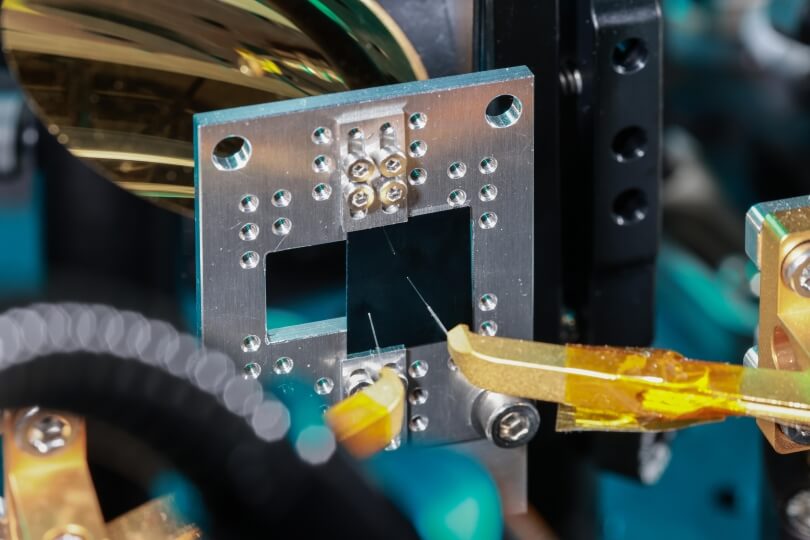
The HYLAB's chip with integrated photonic circuit made of lithium niobate. (Alain Herzog)
Researchers at the Harvard John A. Paulson School of Engineering and Applied Sciences (SEAS), in collaboration with Cristina Benea-Chelmus at the Laboratory of Hybrid Photonics (HYLAB) in EPFL’s School of Engineering, and ETH Zurich, have developed a new thin-film circuit that, when connected to a laser beam, produces finely tailorable terahertz-frequency waves. The device opens up a world of potential applications in optics and telecommunications by exploiting the so-called terahertz gap, which lies between about 300-30,000 gigahertz on the electromagnetic spectrum. This range is currently something of a technological dead zone, describing frequencies that are too fast for today’s electronics and telecommunications devices, but too slow for optics and imaging applications.
Thanks to an extremely thin chip with an integrated photonic circuit made of lithium niobate, SEAS researchers and colleagues at HYLAB and ETH Zurich have succeeded not just in producing terahertz waves, but in engineering a solution for custom-tailoring their frequency, wavelength, amplitude, and phase. Such precise control over terahertz radiation means that it can now potentially be harnessed for next-generation applications in both the electronic and optical realms. The results have recently been published in Nature Communications.
“This was made possible due to the unique features of lithium niobate integrated photonics,” said co-first author Amirhassan Shams-Ansari, a postdoctoral fellow at the SEAS Laboratory for Nanoscale Optics, led by Marko Lončar, Tiantsai Lin Professor of Electrical Engineering and Applied Physics.
Terahertz waves have been produced in a lab setting before, but previous approaches have relied primarily on bulk crystals to generate the right frequencies. The use of the lithium niobate circuit, finely etched at the nanometer scale by collaborators at Harvard University, makes their novel approach much more streamlined. The use of a silicon substrate also makes the device suitable for integration into electronic and optical systems.
To achieve this, Benea-Chelmus’ lab designed the chip’s arrangement of channels called waveguides, from which microscopic antennas broadcast terahertz waves generated by light from optical fibers. This has particular potential for miniaturized lithium niobate chips in spectroscopy and imaging, as terahertz waves are much lower-energy than many other types of waves (like x-rays) currently used to provide information about the composition of a material – whether it’s a bone or an oil painting.
Cutting-edge science delivered direct to your inbox.
Join the Harvard SEAS mailing list.