News
The Research Experience for Undergraduates brings students from numerous universities around the country to the Harvard John A. Paulson School of Engineering and Applied Sciences (SEAS). Students live on campus for 10 weeks while engaging in multidisciplinary laboratory research with a wide range of SEAS faculty. Once they return to their own campuses in the fall, the students then build on their hands-on experiences of doing research here, often causing a ripple effect that benefits not just the individual students, but engineering and computer science departments around the country.
This year saw 24 students representing 15 different colleges and universities spend their summer researching at SEAS. Alongside the traditional oral presentation and research poster at the end of the program, the 2025 REU cohort also took on communications projects designed to explain their research to a general audience. These projects could be done through a range of media, including written blog posts or videos.
Lysis-Driven Transformations in Microbial Active Matter
By Kevin Wang
Kevin Wang, a rising junior biomedical engineering major at Boston University, presents his REU 2025 project, "Lysis-Driven Transformations in Microbial Active Matter"
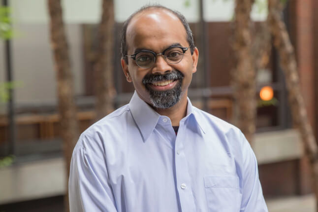
Lana Azar is a rising senior at the University of California-Santa Barbara, majoring in computer science and mathematics. With funding from the National Science Foundation’s Engineering Research Center for Quantum Networks, Azar spent the summer in the labs of Marko Loncar, Tiantsai Lin Professor of Electrical Engineering, and Evelyn Hu, Tarr-Coyne Professor of Applied Physics and of Electrical Engineering. Her research project, “Scalable integration of silicon G-centers with slow-light photonic crystal cavities for quantum photonics,” was also advised by Chaoshen Zhang, a quantum science and engineering Ph.D. student in the Hu Research Group.
Read below to learn more about Azar’s research and summer experience.
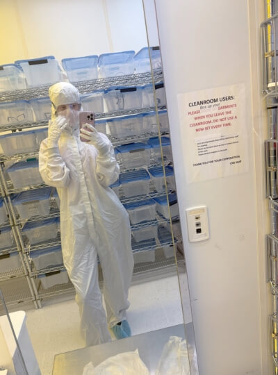
Lana Azar, rising senior computer science and mathematics major at the University of California-Santa Barbara, in her cleanroom suit at SEAS
Finding Light in Silicon: My Summer at Harvard
By Lana Azar
When I first applied to Harvard’s summer research program, I wasn’t exactly expecting that I would be accepted. I worried I wouldn’t know enough, wouldn’t be good enough, wouldn’t belong. I come from a background where access to cutting-edge research isn’t a given, and suddenly I was being offered a chance to work on something that sounded like science fiction: quantum communication and photonic crystals. I accepted the offer with excitement and anxiety bundled together.
This summer, I joined Dr. Marko Loncar’s and Dr. Evelyn Hu’s labs working on something called “silicon G-centers” – tiny imperfections in silicon that can emit single particles of light (photons). Why does this matter? Because in the world of quantum communication and computing, photons are the messengers. They carry quantum information, and if we can control them precisely, we can build technologies that are exponentially faster and more secure than what we have today.
But there’s a catch. These photon-emitting defects don’t naturally behave well. They’re finicky, hard to place precisely, and often don’t emit light efficiently. That’s where my project comes in.
Making Defects Shine
Imagine you're trying to whisper into a canyon and hoping someone across the valley hears you clearly. Not ideal, right? Now imagine you're whispering into a perfectly tuned echo chamber - it amplifies your voice and directs it exactly where it needs to go. That’s what we’re trying to do with these silicon G-centers: embed them in tiny optical cavities (structures that trap and direct light) to make them emit photons more efficiently and predictably.
But placing these defects precisely inside those cavities is extremely hard. Traditional techniques used in diamond (another material often used in quantum tech) don’t work as well in silicon because the process is messier and involves more steps. It’s like trying to do surgery blindfolded.
So we’re taking a different approach: instead of demanding perfection in placement, we’re designing “slow-light” photonic crystal cavities that are more forgiving. These structures slow down light in a controlled way, so even if the defect isn’t placed exactly at the center, it still interacts strongly with the light field. It’s a clever workaround, one that could make quantum devices in silicon more practical and scalable.
What I Actually Do All Day
My project is split into two main parts: simulation and fabrication. In the first part, I use a software tool called Tidy3D to design and simulate the behavior of these photonic crystal cavities. It’s a bit like virtual LEGO, except instead of building castles, I’m building nanoscale light traps and tuning their properties until I get the behavior I want - maximum light amplification and compatibility with silicon.
Once the design is optimized, the second part kicks in: actually building the device. This involves learning to use electron beam lithography, spinning resist onto wafers, etching patterns with ions, and examining the results under high-resolution microscopes. It’s exacting work, and honestly, kind of thrilling. I’m literally shaping light at the nanoscale.
Here are two more videos produced by REU students this summer.
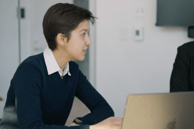
High throughput intracellular delivery
By Emma Vinokour
Emma Vinokour, a rising junior biological sciences major at Northwestern University, presents her REU 2025 project, "High throughput intracellular delivery"
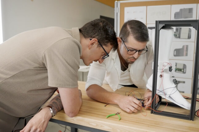
Analyzing Structural Contributions of 3D-Printed Porous Electrodes
By Khoi Bui
Khoi Bui, a rising junior mechanical engineering major at the University of California-Berkeley, presents his REU 2025 project, "Analyzing Structural Contributions of 3D-Printed Porous Electrodes"
Topics: Academics, Applied Physics, Bioengineering, Materials Science & Mechanical Engineering
Cutting-edge science delivered direct to your inbox.
Join the Harvard SEAS mailing list.
Press Contact
Matt Goisman | mgoisman@g.harvard.edu