News
Key Takeaways
- SEAS and physics researchers report a new way to make ultra-smooth, microscopic mirrors that form high-performance optical resonators, or cavities.
- The technique harnesses silicon’s inherent properties and mechanical stress from thin dielectric coatings for the mirror to buckle into shape.
- The optical cavities could become components of quantum networks and other applications.
Researchers in the Harvard John A. Paulson School of Engineering and Applied Sciences (SEAS) and the Faculty of Arts and Sciences have devised a new way to make some of the smallest, smoothest mirrors ever created for controlling single particles of light, known as photons. These mirrors could play key roles in future quantum computers, quantum networks, integrated lasers, environmental sensing equipment, and more.
A team from the labs of Marko Lončar, the Tiantsai Lin Professor of Electrical Engineering at SEAS; Mikhail Lukin, the Joshua and Beth Friedman University Professor in the Department of Physics; and Kiyoul Yang, assistant professor of electrical engineering at SEAS; have published in Optica about their new method for making high-performance, curved optical mirrors. Using two such mirrors to trap light between them, the team demonstrated state-of-the-art optical resonators that can control light at near-infrared wavelengths, which is important for manipulating single atoms in quantum computing applications.
Optical resonators, also known as optical cavities, are fundamental building blocks of countless light-based devices today, from precision instruments for timekeeping and spectroscopy, to lasers and optical interconnects in data centers. They are like guitar strings, but for light: Only certain wavelengths of light (as opposed to sounds) can fit inside the space between two mirrors and intensify. Increasingly, quantum applications require these same types of optical cavities, but much smaller and with lower signal loss.
The Harvard team’s new microfabrication method, led by first author and former graduate student Sophie Ding, was inspired by a practical problem facing colleagues in experimental physics who are trying to build quantum networks out of ultracold single atoms. They were in search of optical cavities with extremely smooth mirrors that would strongly couple atoms to photons, work at specific wavelengths, and could be scaled and shaped.
“We needed these high-quality photonic interfaces to create efficient ways to have single photons interact with single atoms, allowing for fast, high-fidelity quantum networking,” said paper co-author Brandon Grinkemeyer, a postdoctoral researcher in the Lukin lab.
But most lithography or etching methods today cannot produce sufficiently smooth mirror surfaces for the most demanding quantum applications.
Ding’s new method is an example of working smarter, not harder.
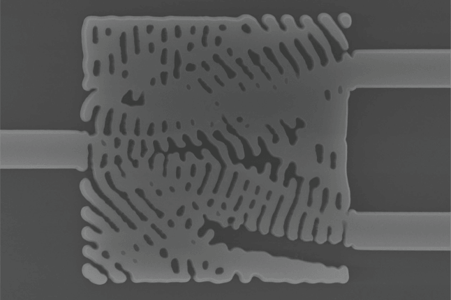
The researchers started with a silicon wafer and used thermal oxidation to grow a thin layer of silicon oxide on the surface, which works to flatten bumps and grooves. When removed, the oxide leaves behind a smooth silicon surface. On that surface, the researchers deposited a precisely engineered stack of transparent oxide layers, called a dielectric mirror coating. When a hole is etched through the back and the coating is freed from the silicon wafer, it buckles into a perfectly curved shape because of built-in mechanical stress, that naturally forms a high-quality mirror.
This process allows the researchers to control the radius of the mirror’s curvature and the wavelengths of light the mirror will reflect, making the method highly scalable and relatively simple.
“In microfabrication, we are sometimes confined by the thought that surface roughness is defined by the etch or the mask, and we try very hard to optimize them,” Ding said. “But when we are using the properties of the materials, we can do a lot less of that and have more robust results.”
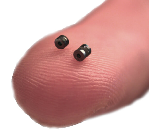
Microcavities of two different lengths, 45 microns and 1 millimeter, placed on a finger tip.
The researchers showed their microfabricated resonators could reach a record “finesse” of 0.9 million at a wavelength of 780 nanometers, meaning light can bounce back and forth inside the cavity nearly a million times before scattering. By contrast, optical telecommunications signals transmit at 1550 nanometer wavelengths.
The optical cavities created with Ding’s new method could be used in modular quantum computing applications, in which many atoms are linked together by photons in optical fibers. The cavities would be the critical interfaces that let an atom’s quantum state be converted into light, transmitted, and written back into another atom.
The potential impact of the work extends beyond quantum computing. Due to its versatility and scalability, it could be adapted for other wavelengths that serve ultra-compact lasers, spectroscopic sensors, and integrated photonics in which many optical resonators can be built directly onto chips.
The paper was co-authored by G.E. Mandopoulou, R. Jiang, A.S. Zibrov, G. Huang, K. Yang, and M.D. Lukin. The work was supported by the U.S. Department of Energy, the National Science Foundation, the Center for Ultracold Atoms, and the Air Force Office of Scientific Research. The fabrication was done at the Center for Nanoscale Systems at Harvard, also supported by the National Science Foundation.
Topics: Materials Science & Mechanical Engineering, Optics / Photonics, Quantum Engineering, Research, Technology
Cutting-edge science delivered direct to your inbox.
Join the Harvard SEAS mailing list.
Scientist Profiles
Marko Lončar
Tiantsai Lin Professor of Electrical Engineering
Press Contact
Anne J. Manning | amanning@seas.harvard.edu