News
Key Takeaways
- Harvard SEAS researchers have found that silica, long thought to lack the right properties for optical metasurfaces, can sometimes outperform standard high-index materials like titanium dioxide.
- Because silica is compatible with large-scale chip-making processes, the insight opens a path to scalable and robust flat optical devices.
An unexpected discovery in a Harvard lab has led to a breakthrough insight into choosing an unconventional material, silica, to make optical metasurfaces – ultra-thin, flat structures that control light at the nanoscale and are already replacing traditional optical devices like lenses and mirrors.
A team from the lab of Federico Capasso, the Robert L. Wallace Professor of Applied Physics and Vinton Hayes Senior Research Fellow in Electrical Engineering in the John A. Paulson School of Engineering and Applied Sciences (SEAS), and collaborators at the University of Lisbon led by professor Marco Piccardo, has found that in some cases, silica — the fundamental building block of glass — can be used for making metasurfaces despite long-held assumptions that it cannot bend light sufficiently for more specialized meta-optics. The research is published in Nano Letters.
Metasurfaces are flat, compact devices patterned with nanoscale structures that look like tiny pillars, each of which is precisely engineered to influence light. Capasso’s team at Harvard was among the first to explore the extraordinary physics of visible-spectrum metasurfaces and their potential to revolutionize things like cameras, microscopes, sensors, and communication systems.
Conventional wisdom: High refractive index is better
As the field of meta-optics has grown, conventional wisdom has pointed to certain classes of materials as ideal for controlling light at this scale. Most favored are materials with what’s called a high refractive index – those that can strongly slow and bend light and that offer full control over light’s phases. Titanium dioxide is a favorite, because it’s transparent and doesn’t absorb much light. Silicon is another, because of its high refraction and ease of fabrication.
One other transparent and widely understood material, silica, a.k.a. silicon dioxide, has generally been considered less desirable for metasurfaces because it has a relatively low refractive index, or a more gentle effect on light. Yet, silica offers intriguing advantages – it can handle high-powered lasers without damage, and it is fully compatible with large-scale chip-making processes.
In the lab one day, first author Luca Sacchi was measuring some fabricated samples of metasurfaces made out of silica. He noticed that the samples, riddled with imperfections, nonetheless performed “remarkably well” across many wavelengths of light, acting just like a lens, Sacchi recalled.
“It was kind of weird, and a bit unexpected,” said Sacchi, a research fellow with Capasso’s lab at Harvard. “If the same thing would’ve been done with a high-refractive index material, like titanium dioxide, it would’ve behaved differently.”
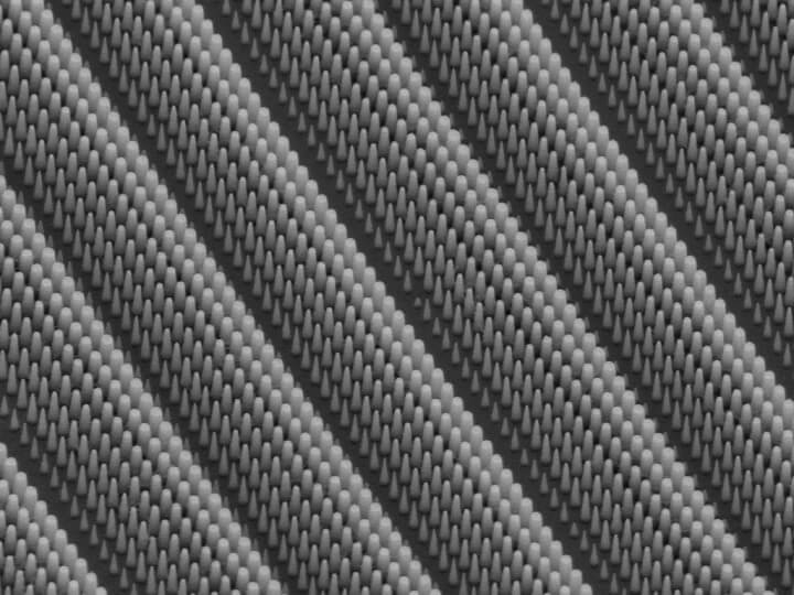
Scanning electron microscopy image of an "imperfect" silica metasurface fabricated at Harvard, in which the final nanopillar shapes are not the desired cylindrical geometry.
Wanting to learn more about their “imperfect” silica metasurface, they teamed up with former Capasso group member Piccardo, now at University of Lisbon, whose lab specializes in a particular nanoscale fabrication protocol that could create silica metasurfaces to exact specifications.
After working with the Lisbon partners to create experimental samples and testing them in the lab at Harvard, the researchers concluded that a hidden feature of low-index materials like silica is that they behave as metasurfaces if the geometry of each nanopillar is carefully considered.
“Moreover, we started to understand exactly when, in the design space of these optical metasurfaces, one should use low-index materials, rather than high-index materials,” Sacchi said.
Single-mode nanopillars
The researchers report in Nano Letters that lower-index materials, or those that do not significantly refract light, nonetheless can out-perform high-index materials that have more commonly been used for metasurfaces, because in low-index materials like silica, each etched nanopillar supports only a single, clean path of light.
In this “single-mode” regime that does not suffer from interference between light modes because the light is not split into multiple paths, the desired phase profile and transmission of light can be achieved. The result is that lower-index materials allow for efficient design of devices with more relaxed feature sizes – wider nanopillars, and larger spaces between them, relative to the wavelength of light.
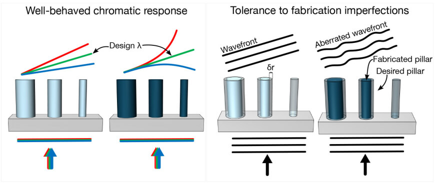
A figure that outlines the advantages of low refractive index metasurfaces.
That’s important when thinking about metasurfaces in the real world: If in certain instances, glass or silica metasurfaces would perform best, they could be made with standard tools like photolithography, as opposed to the more expensive and time-consuming electron beam lithography, lowering costs and integrating into existing chip-making processes. The researchers also showed that silica metasurfaces may be more forgiving of fabrication errors, further underscoring their potential for commercial devices.
“The advantages of silica meta-optics we highlight here were partly overlooked until now because of major obstacles in nanofabrication,” Piccardo said. “As we are able now to etch very tall nanopillars with vertical sidewalls, we can make full use of this low-index platform, with all its benefits for exciting applications. Low-index metasurfaces inherently provide two key benefits: a broad, well-behaved chromatic response without the need for complex dispersion engineering, and a robustness to fabrication errors, which is exactly what our initial curiosity set out to understand.”
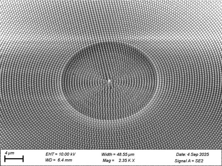
Scanning electron microscopy image of a silica metasurface fabricated at University of Lisbon, with no visible imperfections and tall, cylindrical nanopillars.
Sacchi, now a researcher at University of California Berkeley, said that the results challenge common misconceptions about metasurface materials and are a good reminder that “it’s better always to question your assumptions.”
Capasso called the discovery “a counterintuitive breakthrough in nanotechnology.”
“We have demonstrated in one sweep many high-performance flat optical devices – lenses, gratings, and phase plates – using low-refractive index materials, potentially providing a route to scalable and fabrication error-resilient flat optics,” Capasso said.
The paper was co-authored by Alfonso Palmieri, Vitthal Mishra and Joon-Suh Park. The research was performed in part at the Harvard Center for Nanoscale Systems, supported by the National Science Foundation under NSF Award ECCS-2025158. Other support came from the Air Force Office of Scientific Research and the European Research Council.
Topics: Applied Physics, Electrical & Computer Engineering, Materials Science & Mechanical Engineering, Metasurfaces, Optics / Photonics, Research
Cutting-edge science delivered direct to your inbox.
Join the Harvard SEAS mailing list.
Scientist Profiles

Federico Capasso
Robert L. Wallace Professor of Applied Physics and Vinton Hayes Senior Research Fellow in Electrical Engineering
Press Contact
Anne J. Manning | amanning@seas.harvard.edu