News
Key Takeaways
- A Harvard team built a chip-scale lithium niobate UV light source that generates 120 times more power than previous approaches, paving the way for practical uses.
- They used a novel fabrication method called sidewall poling to maximize frequency conversion of red to UV light on the chip.
Ultraviolet light, beyond its natural abundance from the sun, is used in countless modern applications, from disinfection, to fluorescence of biological materials, to photolithography of computer chips. In the near future, pinpricks of UV light on photonic chips are expected to drive advances in quantum computers, ultra-precise atomic clocks, and more.
But sufficiently compactifying UV light sources to this degree is no easy task, as this type of light tends to lose power rapidly as it travels along optical waveguides, stymying any meaningful attempts at chip-scale light sources at this wavelength — until now.
Using a workhorse photonic platform called thin-film lithium niobate, a Harvard-led team from the lab of Marko Lončar, the Tiantsai Lin Professor of Electrical Engineering, has demonstrated a micron-scale photonic device that generates two orders of magnitude more UV light on a chip than previous comparable approaches. The research, published in Nature Communications, paints lithium niobate as a viable platform for high-power, low-loss, compact UV light generation for practical applications.
The new device circumvents the difficult task of delivering UV light at this scale by converting red light to UV light on-chip. In this process, known as frequency upconversion, two red photons combine inside the lithium niobate crystal, which has extremely efficient frequency-conversion abilities, to create one higher-energy UV photon.
“Our group is perhaps best known for utilizing lithium niobate for photonic devices that operate at longer, infrared wavelengths – closer to the realm of telecommunications signals,” Lončar said. But it turns out this transparent, crystalline material that’s become a star platform for integrated photonics can also effectively guide and host light sources at the shorter wavelengths including UV, he continued.
“When people think about [thin-film lithium niobate], they don’t think of it as a UV material, but we show that it is,” said co-first author Kees Franken, former research fellow in the Lončar lab. “We also show that there are some other nonlinear effects happening that we don’t fully understand yet.”
New method: Sidewall poling
In the device, light is guided through the chip in waveguides — microscopic “wires” for light etched into the film. To efficiently convert red light to UV, the crystal grain structures in lithium niobate must be periodically flipped and evenly spaced along the waveguide — a specialized nanofabrication process for nonlinear optics known as poling. Getting that pattern exactly right, on sub‑micron length scales over centimeter‑long devices, is what has limited previous attempts.
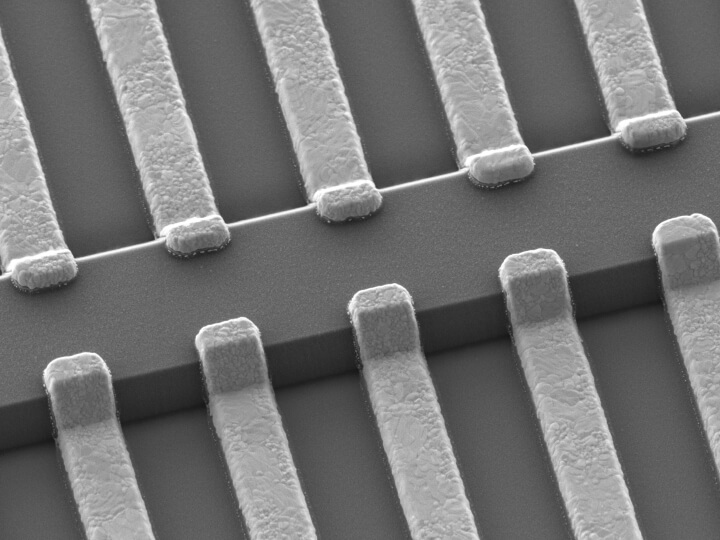
Scanning electron microscope image of metal electrodes used for sidewall poling.
Earlier approaches faced a tradeoff: You could pole the entire film but lose the ability to compensate for fabrication imperfections. Or, you could fabricate the waveguides first, but at the cost of efficiency due to far-away placement of electrodes and only partial poling of the film.
The Harvard team overcame this tradeoff by inventing “sidewall poling.”
Instead of placing poling electrodes only above the film, they brought carefully patterned metal “fingers” right up to the sides of the etched waveguide, or its sidewalls. Then, in line with existing techniques, they applied a small voltage during fabrication to permanently flip the crystal domains in a tightly controlled pattern.
“The key idea was: could we just put the electrodes directly on the waveguide?” said co-first author and former graduate student Soumya Ghosh. “It’s a high-precision fabrication process to position the electrodes but requiring about 50-nanometer accuracy.”
This unique electrode geometry allowed the researchers to fully invert the crystal across the entire waveguide cross‑section, so the light sees a perfectly flipped material, and conversion efficiency is maximized. Also, they could precisely tailor the poling period along the device, using earlier “adapted poling” techniques developed in the Lončar lab and other places, to overcome variations in film thickness and waveguide shape.
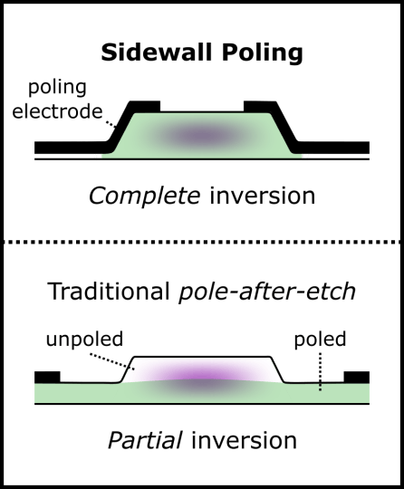
Schematic showing the benefit of sidewall poling vs. traditional pole-after-etch methods.
Results show increased power output
In their paper, the team reports 4.2 milliwatts of on‑chip UV power at 390 nanometers wavelength – about 120 times more output power than the previous best thin-film lithium niobate demonstrations in this wavelength range. Earlier demonstrations with this material produced only tens of microwatts of UV power, which was enough to show that the concept worked, but far too little for anything practical.
High‑quality, chip-scale UV light is particularly important for emerging technologies like trapped‑ion quantum computers, where specific atomic transitions often lie in the near‑UV range.
“If you want a scalable quantum computer that isn’t the size of a truck, you need to scale everything down to the chip level, and this includes the light sources,” Franken said.
Beyond quantum and timing applications, the same wavelength band is attractive for compact environmental sensors for close monitoring of greenhouse gases or other atmospheric pollutants, the researchers added.
According to Franken and Ghosh, the advance was possible because Lončar’s group integrates all aspects of the work, from theory and design to cleanroom fabrication and optical testing, under one roof.
“The hands-on intuition that we gained for how to make a device, while also keeping the zoomed-out view of what this device is for, and how we were going to characterize it – that’s a big part of what enabled this project for us,” Ghosh said.
“Milliwatt-level UV generation using sidewall poled lithium niobate” was further co-authored by C.C. Rodrigues, J. Yang, C.J. Xin, S. Lu, D. Witt, G. Joe, G.S. Wiederhecker, and K.-J. Boller. U.S. federal funding for the project came from the following sources: Department of the Air Force grant No. FA9453-23-C-A039; Office of Naval Research grant No. N00014-22-C-1041/VAS-21-0001; NASA grant No. 80NSSC22K0262 and 80NSSC23PB442; and National Science Foundation grants ERC EEC-1941583 and OMA-2137723.
Topics: Applied Physics, Electrical & Computer Engineering, Materials, Optics / Photonics, Research, Technology
Cutting-edge science delivered direct to your inbox.
Join the Harvard SEAS mailing list.
Scientist Profiles

Marko Lončar
Tiantsai Lin Professor of Electrical Engineering
Press Contact
Anne J. Manning | amanning@seas.harvard.edu